Precision for the Semiconductor Industry
High-quality wafer marking and sorting systems for globally renowned semiconductor manufacturers.
Trusted by globally renowned wafer and chip manufacturers
Years of Experience
Since 1995, InnoLas Semiconductor has been developing high-quality machines for wafer marking & wafer sorting of semiconductor materials, thus possessing decades of industry expertise.
International Locations
With its headquarters in Germany and locations in Singapore and Croatia, InnoLas is positioned internationally. We also work with experienced distributors who support customers in target markets with sales and service expertise.
Cleanroom Production
Manufacturing and commissioning take place in our own cleanroom environment. This creates clean working conditions and supports the highest quality requirements of our customers.
Employees
Our company has a highly qualified team of experienced specialists. Through continuous training, profound expertise, and many years of practical experience, we ensure that we can always offer our customers solutions of the highest standard.
kWh of solar power per year
With our 60 kWp solar system, we generate more than 40% of our electricity needs ourselves. This reduces our energy consumption from external sources and actively contributes to more sustainable and resource-efficient production. In this way, we combine economic action with ecological responsibility and specifically invest in a sustainable future.
Our Solutions
for the world’s leading semiconductor manufacturers.
-
Wafer Marking
Our Wafer Marking enables permanent, high-precision, and particle-free marking of wafers for seamless traceability in semiconductor production.
Learn More -
Wafer Sorting
Our Wafer Sorting enables reliable, automated sorting and classification of wafers for efficient and transparent semiconductor production.
Learn More -
EFEM & Inspection
We offer suitable automation for inspection and measurement applications, always adapted to our customers' needs.
Learn More -
HighQ Components
highQ Components is a brand of InnoLas Semiconductor GmbH and distributes laser safety components, such as shutters or fiber laser safety modules.
Learn More
Systems
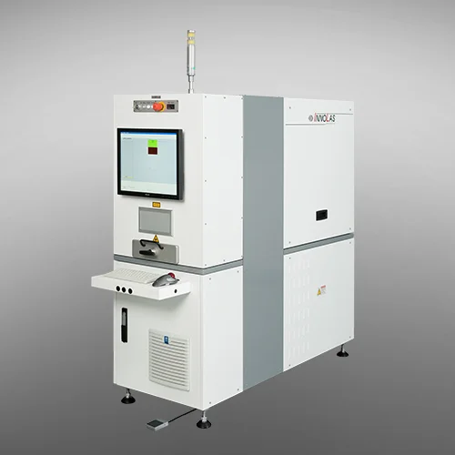
Specially developed laser technology for the highest quality on all wafer materials.
IL 600
- Manual Handling
- Wafer holder for various wafers
- Suitable for low volume
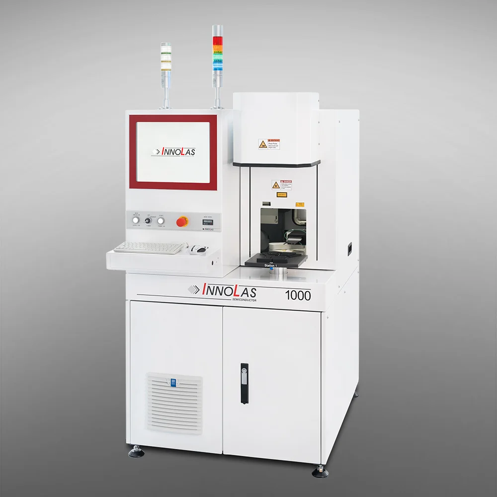
IL 1000
- Automatic Handling
- One load station
- Small footprint required
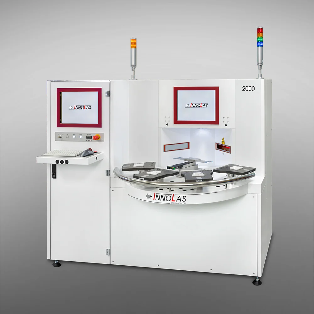
IL 2000
- Automatic Handling
- Four load stations
- Also configurable with sorting function
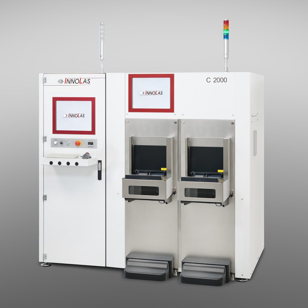
IL C2000
- Automatic Handling
- Up to three load stations
- ISO 3 Minienvironment
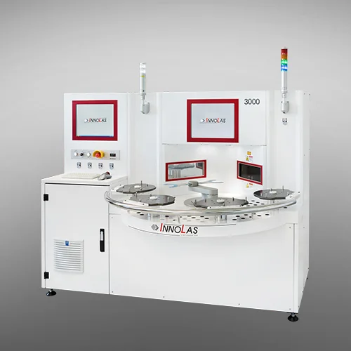
IL 3000
- Hard Marking of unpolished wafers
- Suitable for manual loading
- Four load stations
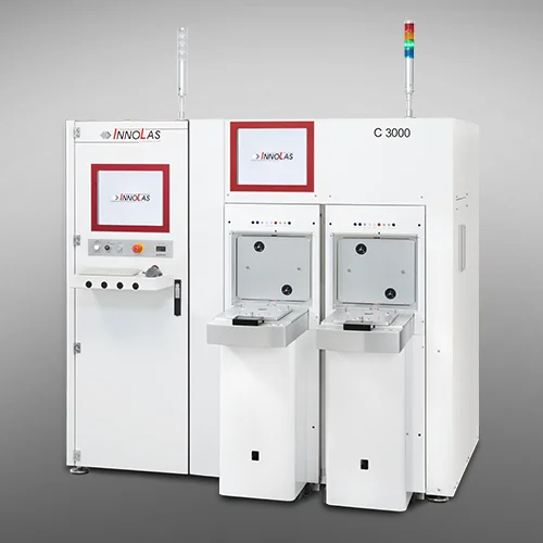
IL C3000
- Soft Marking of polished wafers
- Suitable for AGV/OHT loading via E84
- ISO 3 Minienvironment
IL D3000
- Hard Marking of unpolished wafers
- Suitable for AGV/OHT loading via E84
- Fan Filter Units optional
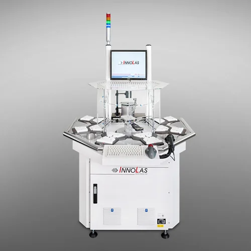
IL 2600
- Sorting by ID, weight & thickness
- High throughput up to 250 wafers per hour
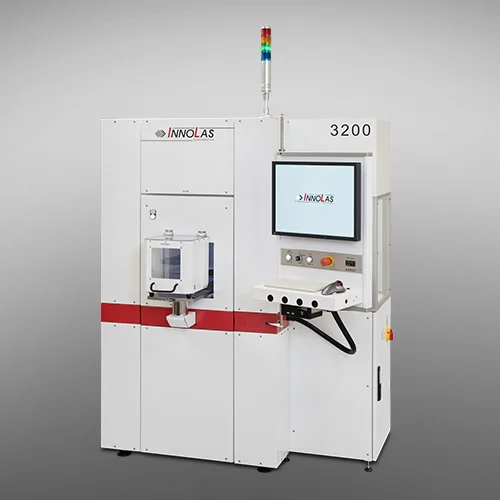
IL C3200
- Sorting by ID or inspection result
- Suitable for AGV/OHT loading
- ISO 3 Minienvironment available
IL C3600
- Sorting by ID or inspection result
- Suitable for AGV/OHT loading
- ISO 3 Minienvironment available
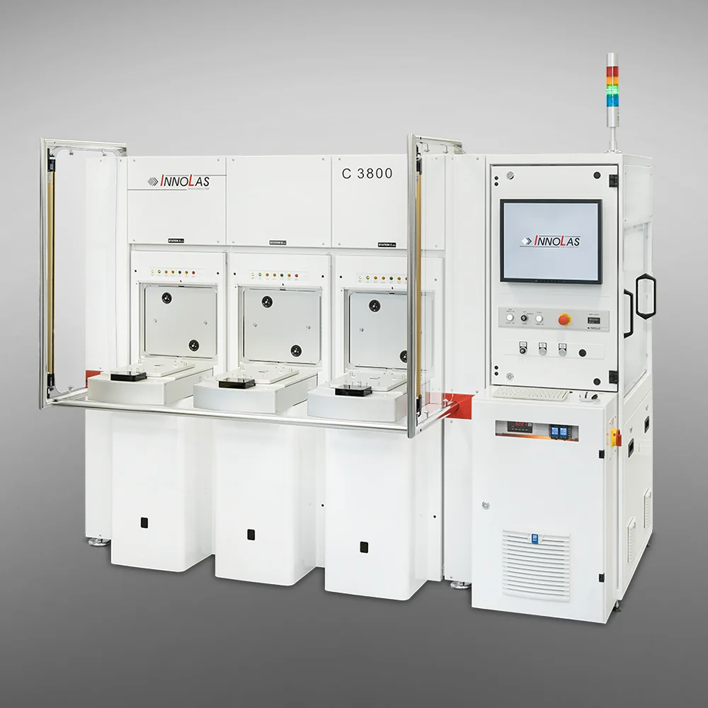
IL C3800
- Sorting by ID or inspection result
- Suitable for AGV/OHT loading
- ISO 3 Minienvironment available
Quality - Made in Germany
For over 30 years, we have been developing and manufacturing high-precision special machines for the world’s leading semiconductor manufacturers at our headquarters in Inning am Ammersee.
Specialist in the Semiconductor Industry
For decades, we have focused on wafer marking and sorting, and the automation of inspection modules.
Customized Solutions instead of Standard Machines
Every customer has different requirements. We meet these with individual platforms and a variety of optional features.
Innovation & Technology
The continuous further development of our systems and components, as well as our high vertical integration, distinguish us.
Worldwide Customer Support
Experts with decades of industry experience and extensive knowledge are located worldwide close to our customers' production sites to ensure immediate support.
News & Updates
always stay up to date…
Consultation & Configuration
From the initial requirements analysis to the successful final acceptance of your wafer marking or wafer sorting system, a personal contact person will accompany you – for a solution precisely tailored to your manufacturing requirements.
InnoLas Wafer Marking Systems offer maximum precision, cleanroom suitability, and full traceability for efficient, stable semiconductor processes.
InnoLas Sales Team