
Wafer Inspection
InnoLas Wafer Inspection detects scratches, particles, edge defects and cracks fully automatically – on the front and back of the wafer, at the edge and after dicing. Our EFEM platforms reliably transfer the wafers to the inspection module; depending on the inspection result, they are then processed further or sorted out.
- SEMI-compliant
- Reproducible results
- All wafer sizes
Many inspection types – one interface
Our wafer inspection systems offer five core processes that can be configured individually and ensure end-to-end process control in semiconductor manufacturing.
Wafer Front and Back Side
Surface inspection with multispectral illumination
Detecting defects before they become a problem – that is the core of our AOI wafer inspection solutions. Our systems reliably capture the full spectrum of typical defect patterns: from surface defects such as scratches, particles and inclusions, to structural defects such as microcracks, chipping and delamination, through to process-related deviations from CMP, lithography, etching and deposition. This gives you not only complete quality assurance, but also valuable process data for the continuous optimization of your production.
Detection
MultiView technology
Throughput
up to 180 wph
Configuration
Manual to fully automated
Capabilities:
- Automatic sorting into good, rework or scrap
- Edge scan can be combined in one EFEM
- Reduces costs and increases production yield
Detectable defects:
Wafer Edge
360° edge inspection with rotating module
The wafer edge is mechanically highly exposed and a frequent starting point for microcracks, chipping and particle contamination. Our wafer edge inspection covers the entire wafer bevel – from the top edge across the apex to the bottom edge, as well as notch and flat – seamlessly from every angle. Defects such as chipping, cracks and scratches are detected early, before they lead to wafer breakage in the tool or contaminate subsequent process steps. The result: less scrap, higher yield and reliably protected production equipment – with the InnoLas Wafer Inspection solution.
Measurement technology
Line scan camera technology
Process time
15 seconds
Result display
Wrap-Around Multiview
Your advantages:
- Simultaneous inspection of front surface, bevels (front/back bevel), shoulders, apex and back side in a single scan.
- High precision at high speed – pixel resolution of approx. 3 μm at scan speeds of up to 60 mm/s
- Seamless system integration – uses the integrated wafer pre-aligner, SEMI-compliant and controllable via GUI
Detectable defects:
Cracks After Dicing
Optical crack inspection with inking & automatic sorting
An optical measuring device detects local cracks and defects after dicing. Brittle bonding materials in particular are prone to invisible microcracks that can arise during wafering, front-end or back-end processes and put entire process chains at risk. Defective chips are “inked” (marked) and sorted out by a pick-and-place robot in the next process step. This significantly reduces scrap and substantially increases yield.
Measurement technology
Precision sensors
Image acquisition
On the fly
Scan position
Top and bottom side
Your advantages:
- High-resolution multiview image acquisition – up to 6 fully synchronized images per wafer
- High speed at full inspection depth – over 100 wafers per hour at 100% inspection (8" wafers)
- Intelligent evaluation without over-rejection – integrated, finely adjustable thresholds and crack characteristics
Detectable defects:
Wafer sorting by thickness or mass – precise measurement with high-accuracy sensors
The thickness or mass of each wafer is measured with high-precision sensors so that subsequent steps in the production process can be adjusted individually. This wafer sorting method groups wafers by thickness or mass tolerances, so that subsequent process steps always work with homogeneous material properties.
Precision weighing technology
200 – 1500 µm
Ascending/descending, groups
Your advantages:
- Individual adjustment of subsequent process steps to wafer thickness/mass
- Sorting in ascending, descending or randomized order
- Homogeneous lots for consistent process results
Suitable for:
Omega/Theta XRD – X-ray diffractometer for precise crystal orientation
The Omega/Theta X-ray diffractometer is a fully automated, vertical three-axis diffractometer for determining crystal orientation at wafer level using the omega scan and theta scan methods as well as rocking curve measurements. With the omega scan method, the complete lattice orientation can be determined in a single crystal rotation of around 5 seconds.
Measurement technology
XRD
Wafer materials
Si, SiC, AlN, GaAs, quartz, LiNbO₃, BBO
Measurement time
6 seconds
Your advantages:
- Ultra-fast crystal orientation measurement – fully automated determination of the complete lattice orientation
- Highest precision – angular resolution of 0.1 arcsec and tilt angle determination with an accuracy of up to 0.001°
- Modular, flexible design – numerous expansion options and individual adaptation to customer requirements
Suitable for:
How fully automated wafer inspection works
From loading the wafer to outputting the results – every step fully automated, reproducible and traceable.
Step 01
Loading
Step 02
Alignment
Step 03
Inspection
Step 04
Classification
Step 05
Result
Why wafer inspection pays off
Defective wafers that pass undetected into subsequent process steps cause scrap, equipment downtime and quality problems. Early inspection prevents this.
↑ Yield
Significant increase through early defect detection
↓ Scrap
Scrap reduction through inking & automatic sorting
100%
Our EFEM as a flexible basis for your wafer inspection solutions
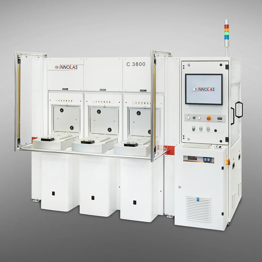
The heart of our wafer inspection solution: the proven Equipment Front End Modules (EFEM) IL C3200, IL C3400 and IL C3800. Scalable to the number of SMIF, FOUP, FOSB or open cassette load ports required, they handle fully automated wafer transfer to the connected inspection or measuring tool – reliably, precisely and with high process reliability. Whether vacuum, edge grip or frame handling: every EFEM is configured exactly to your requirements. With optional extensions such as an ISO 3 mini-environment, a SECS II/GEM interface or customized camera systems, the result is a wafer inspection system that fits perfectly into your production environment – today and in the future.
Which defects do our systems detect?
Scratches & grooves
Particles
Inclusions
Coating defects
Chips & chipping
Edge fractures
Microfractures
Structural damage
Defects in and on the wafer after dicing
Consulting & Configuration
From the initial requirements analysis to the successful acceptance of your wafer inspection system, a dedicated contact person supports you. We help you select the right inspection technology and optics, develop a tailored inspection concept and support feasibility studies as well as the optimal definition of parameters for reproducible results.
InnoLas Sales Team
- Offline or full MES connection via SECS/GEM
- Optional customer-specific interfaces
- Manual or fully automated AGV/OHT loading via E84