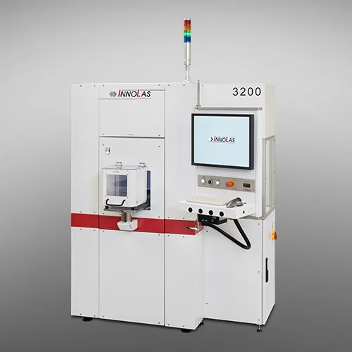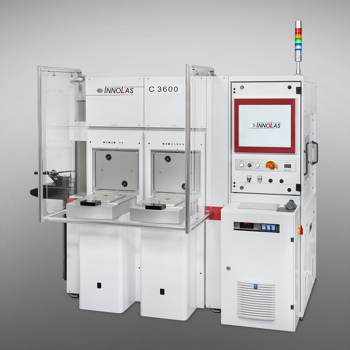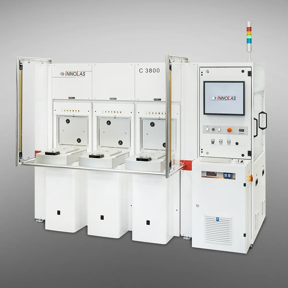
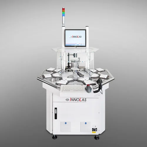
Precise Sorting

Wafer Sorting

In modern semiconductor manufacturing, a smooth, error-free material flow is crucial for efficiency and product quality. Our robust wafer sorters automatically identify and transfer every wafer based on its unique wafer ID – reliably, quickly and with full traceability.

Sorting Processes

Our versatile wafer sorting processes – individual and precise

Our sorters offer four core sorting processes that can be configured individually and ensure end-to-end process control in semiconductor manufacturing.

Sorting by wafer ID – camera-based identification and sorting

In ID-based wafer sorting, the identification code marked on the wafer is read by an integrated camera, and the wafer is then placed in the target carrier according to the code. This wafer sorting method enables end-to-end traceability and targeted assignment of every single wafer in the production process.

Detection

Camera-based

Placement

Recipe- or host-controlled

Traceability

Complete

Capabilities:

Ideal for:

Lot management
Traceability
MES integration
Split & Merge
Randomize

Sorting by wafer mass – precision through high-accuracy weighing technology

A high-precision scale measures the mass of every single wafer so that subsequent steps in the production process can be adjusted individually. This type of wafer sorter ensures that subsequent coating, etching or deposition processes can be optimally matched to the actual wafer mass – for uniform results and increased yield.

Measurement technology

High-precision scale

Accuracy

+/- 0.0001 g

Sorting

Ascending/descending, groups

Your advantages:

Ideal for:

Downstream process adjustment
Coating processes
Yield optimization

Sorting by wafer thickness – precise thickness measurement with high-accuracy optical sensors

The thickness of each wafer is measured with high-precision sensors so that subsequent steps in the production process can be adjusted individually. This wafer sorting method groups wafers by thickness tolerances, so that subsequent process steps always work with homogeneous material properties.

Measurement technology

Optical precision sensors

Accuracy

+/- 0.2 µm

Sorting

Ascending/descending, groups

Your advantages:

Suitable for:

Thickness classification
Polishing/grinding processes
Quality control

Wafer sorting by detected defect in cooperation with third-party inspection tools

Depending on the integrated inspection module, wafers can be precisely classified according to the features to be inspected. The evaluation takes place in real time, so that wafers can be assigned to the corresponding category immediately and transferred automatically to the designated cassette.

Our EFEM systems allow several inspection modules to be integrated within a single process flow. This makes it possible to combine different inspection methods efficiently and increase productivity in the long term.

The result is a reliable, automated, end-to-end process with the highest precision.

Mode

Fully automated

Configuration

Individual

Integration of

Cooperation partners

Your advantages:

Ideal for:

Reproducible measurement results
Increasing yield
Cost reduction
Quality assurance
Consulting & Configuration

Consulting & Configuration

From the initial consultation to the complete machine acceptance of your wafer sorter, a dedicated contact person from our sales team is at your side – for an individual configuration tailored exactly to your requirements.

Global Sales Team

Before delivery, every wafer sorter system undergoes a comprehensive Factory Acceptance Test (FAT), so you can be sure that your system will work reliably and to specification from day one. Our solutions are integrated seamlessly into your existing production environment via SECS/GEM, without disrupting your ongoing operations.

This site is protected by reCAPTCHA and the Google Privacy Policy and Terms of Service apply.

Your Advantages

Our wafer sorting systems deliver

Our customers worldwide are highly specialized semiconductor manufacturing companies that place the highest demands on quality, reliability and flexibility in their production. By using InnoLas wafer sorters, our customers benefit from being able to:

Versatile sorting processes

Individually sort, split, merge or randomize wafers by ID, mass or thickness.

Highest purity

Handle wafers reliably and particle-free under ISO 3 cleanroom conditions.

High throughput

Achieve up to 550 wafers per hour in transfer mode (IL 2600) for maximum productivity.

Flexible handling

Choose between vacuum and edge grip handling – for optimal protection of both wafer sides.

Seamless MES integration

Integrate systems seamlessly with the MES/host via SECS/GEM and load them fully automatically with AGV/OHT via E84.

EFEM cooperation

Use your sorting system as a fully automated loading and unloading system for measurement and inspection tools.
Wafer Handling

Which handling suits your requirements?

Reliable wafer handling is a decisive factor for efficient and stable production processes. Our automated handling systems enable safe, precise and reproducible wafer transport and can be optimally adapted to different process requirements.

With vacuum handling, the wafer is securely picked up and moved by controlled suction. This technology offers high flexibility and can be used for different wafer diameters. This makes it particularly suitable for production environments with different wafer sizes or changing process requirements.

Edge grip handling grips the wafer exclusively at its edge, minimizing contact with the active wafer surface. This method offers advantages for particularly sensitive processes and reduces the risk of contamination or damage. Because the gripper system is designed for a defined wafer diameter, it enables particularly precise and reproducible handling in specialized applications.

Vacuum handling
Edge grip handling
Frame handling
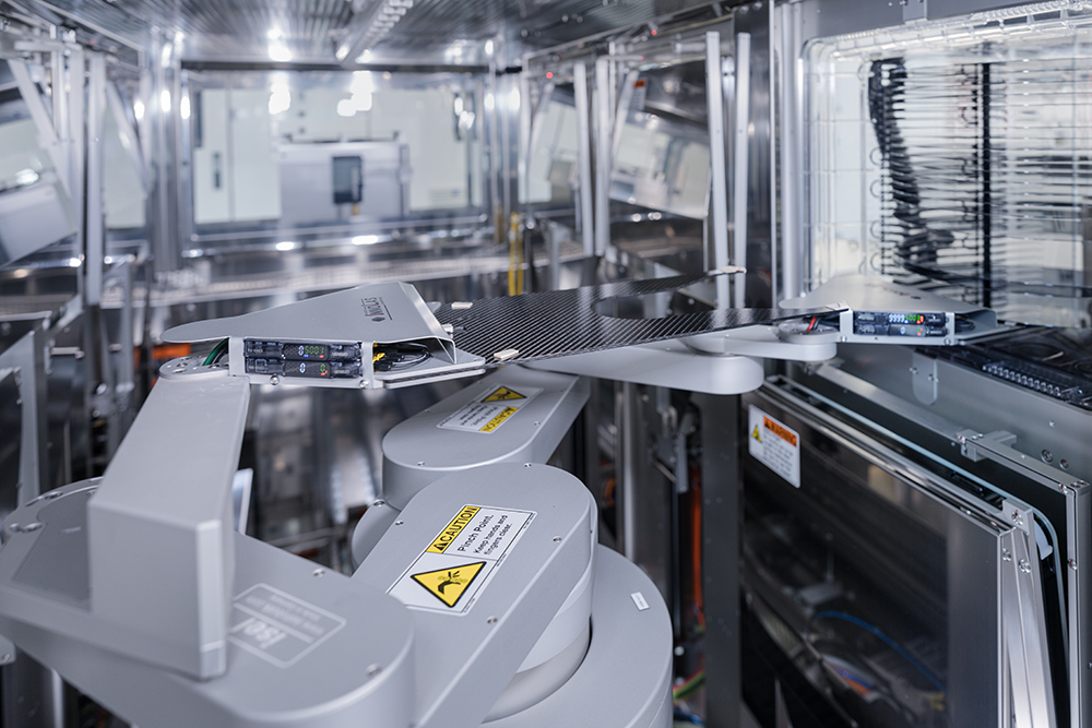
Handling robot inside the IL C3800
Wafer held by the edge grip end effector of the IL C3800
Reinraum einer Halbleiterfertigung mit Anlagenreihen im blauen Licht
Automation

Integration and automation

Our wafer marking systems are designed for seamless integration into automated production lines. The Equipment Front End Module (EFEM) enables standardized connection to a fab’s automated material handling systems (AMHS) via the E84 SEMI standard.

A SECS II/GEM interface enables bidirectional data exchange with common MES systems for production control and quality control.

Reliability & Robustness

High reliability is particularly important

Low-maintenance mechanical components minimize unplanned downtime and make your maintenance predictable. Thanks to fast service access to all modules, the few maintenance tasks on your wafer sorter can be carried out efficiently and quickly.

In addition, we offer a comprehensive service package: from advanced training and worldwide on-site and remote service to log analysis and condition monitoring for early fault detection. Short MTTR times and a worldwide spare parts service ensure maximum system availability and predictable process costs. With InnoLas wafer sorters, you benefit from maximum equipment availability, reduced maintenance effort and optimally predictable operating costs.

Safety & industry standards

Our wafer sorters comply with all relevant standards for semiconductor manufacturing:

CE
NFPA 70, NFPA 79
Optional: SEMI S2/S8
Mini-environments up to ISO class 3
OPC/UA Data Logging
Close to Our Customers

From project start into the future – we are with you all the way

A dedicated contact person accompanies you from the first conversation to the successful completion of the project – with comprehensive technical consulting tailored to your requirements and goals. Together, we identify the optimal wafer sorting platform for your production environment and develop a solution tailored exactly to your process requirements.

Before commissioning, every wafer sorter undergoes a Factory Acceptance Test (FAT) and a Site Acceptance Test (SAT) to ensure a smooth start in your production. Comprehensive training prepares your employees for the safe and competent operation of the system.

We are also at your side after commissioning: with fast on-site and remote support available worldwide as well as regular maintenance – for consistently stable, high-performance production processes with your wafer sorters.

...and they keep an eye on your costs, too!

Through the tailored configuration of robotics, cassette station, options and software modules, your wafer sorter is matched exactly to your production environment – for seamless process integration and maximum cost efficiency from the very start. Thanks to exceptionally long service lives and minimal repair effort, you also benefit from permanently low operating costs during ongoing operation.

Precise handling, uncompromising cleanroom compatibility and a flexible, future-proof system architecture not only ensure reliable processes – they also protect your investment in the long term.

With InnoLas wafer sorters, you benefit from lasting efficiency gains, maximum process reliability and the highest production quality – at optimal cost efficiency. You receive all-round support, maximum system reliability and future-proof solutions for your everyday production.

Two employees checking the wiring of a control cabinet against a plan
Service & Maintenance

Maximum system availability & worldwide service

Our wafer marking systems feature durable, maintenance-free laser sources and optics that ensure uninterrupted marking operation and maximum process reliability. Fast access to maintenance modules and modern remote diagnostics enable early fault detection and preventive maintenance.

A service team available worldwide ensures fast support – on site or remotely. This minimizes downtime and maximizes equipment availability for demanding semiconductor applications.

Flexible sorting solutions for the most demanding production requirements

Whether chip manufacturer or foundry: our wafer sorting solutions fit seamlessly into existing production lines and ensure that every wafer is fed to exactly the right lot, the right route or the right process step. The result is more stable processes, fewer handling errors and complete documentation – from wafer infeed to dicing.

Depending on the model, our wafer sorters process 2″, 3″, 100 mm, 125 mm, 150 mm and 200 mm wafers loaded in open cassettes or SMIF pods. Several solutions are also available for 300 mm wafers, compatible with FOUP or FOSB loading and also suitable for automated loading via overhead transport (OHT) or automated guided vehicle (AGV).

Up to 550 wafers per hour in transfer mode and 250 wafers in sorting mode are possible. High throughput, precise alignment and intelligent control mechanisms enable optimal production – from smaller institutes to 24/7 high-volume production.

InnoLas wafer sorters automate key process steps:

  • Sorting by ID, weight, thickness, defect class or pass/fail criteria
  • Logging and output of the sorting criterion for every wafer. Efficient buffering and sequencing along complex line layouts
  • Gentle handling thanks to advanced vacuum or edge grip handling
+49 8143 24195-0sales@il-semi.comDirectionsPersonal Support