Precision Laser Technology

Wafer Marking with Precision

The unique identification of every single wafer is an essential part of modern semiconductor manufacturing. It ensures complete traceability across all production steps and thus makes a significant contribution to quality assurance and process control.

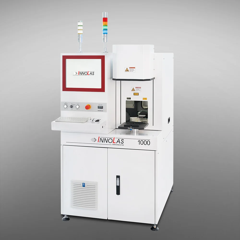
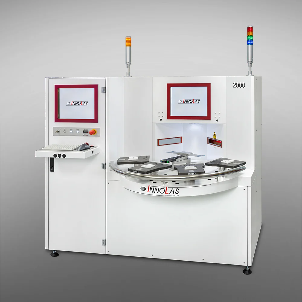
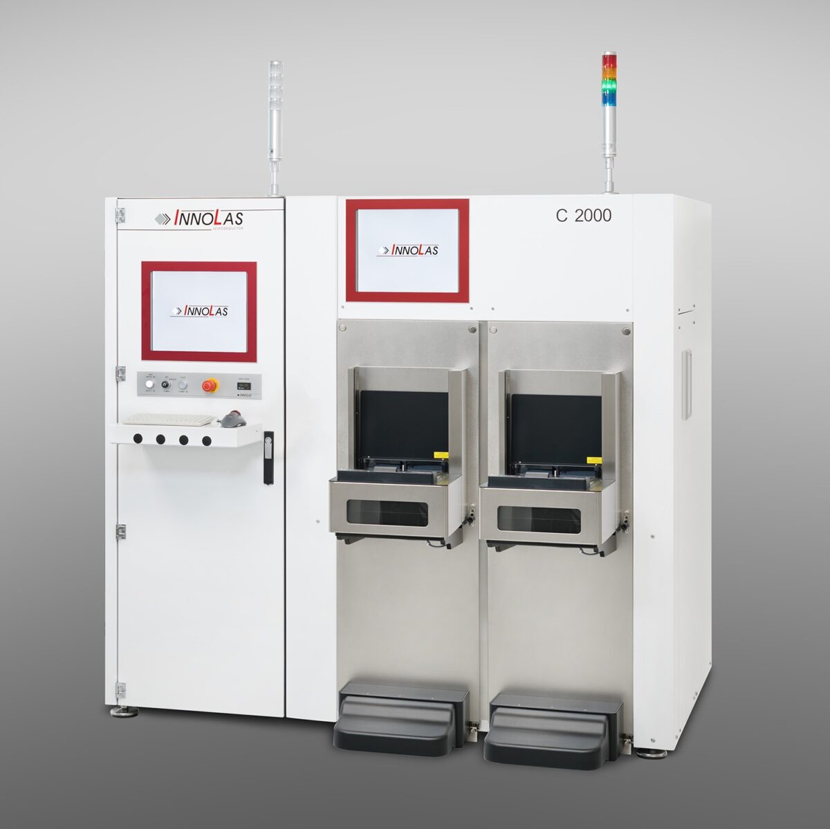
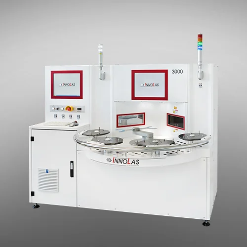
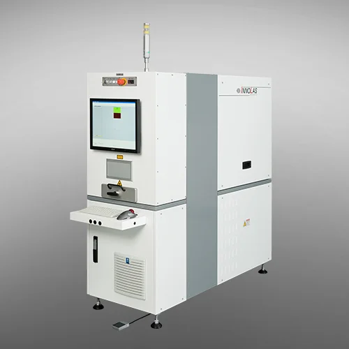
InnoLas supports the world’s leading chip and wafer manufacturers with high-precision, SEMI-compliant marking systems designed specifically for the demanding requirements of the semiconductor industry.

Marking Processes

Which process suits your wafers?

Our systems use advanced laser and galvo scanner technologies, which are indispensable for the two main processes in wafer marking (soft marking and hard marking).

Soft Marking (SML) – precise identification without compromise

For high-quality, polished wafers and EPI surfaces, soft marking is the ideal identification method. With a marking depth of only 0.5 to 5 micrometers, depending on the material, the sensitive wafer surface is subjected to minimal stress – without impairing the electrical or mechanical properties of the material. The particle-free marking result makes soft marking particularly suitable for cleanrooms and therefore the first choice for chip manufacturers who demand both the highest surface quality and complete traceability.

Marking depth

0.5 – 5 µm

Contamination

Particle-free

Process

Material melting

Ideal for:

Polished wafers
EPI surfaces
Front-end processes
Chip manufacturers

Hard Marking (HML) – permanently readable on any surface

Rough, unpolished or mechanically stressed wafer surfaces require a robust identification method that remains reliably readable even under demanding conditions. With material removal of 5 to 100 micrometers, hard marking creates a deep, high-contrast mark that works flawlessly even on sawn, ground or etched surfaces. This makes hard marking the optimal solution for wafer manufacturers who need permanently stable, process-reliable identification along the entire value chain.

Material removal

5 – 100 µm

Contrast

High

Process

Material removal

Ideal for:

Unpolished wafers
Sawn surfaces
Ground wafers
Wafer manufacturers

Lasers used

Our lasers, developed specifically for semiconductor marking, offer maximum stability even under demanding production conditions. With a maintenance-free service life of around 50,000 operating hours, they minimize downtime in wafer marking and sustainably reduce your operating costs. Thanks to state-of-the-art technology, the systems also stand out for their particularly low energy consumption.

Application

Developed for industrial use

Service life

50,000 hours

Operating costs

very low, as maintenance-free

Suitable for:

All semiconductor materials
Soft & Hard Marking
24/7 production
Materials & Wafer Sizes

Supported materials and wafer sizes

Our wafer marking systems support a wide range of wafer materials:

Silicon (Si)
Silicon carbide (SiC)
Gallium nitride (GaN)
Gallium arsenide (GaAs)
SOI wafers
Germanium (Ge)
Glass
Sapphire (Al2O3)
Lithium niobate (LiNbO3)
Lithium tantalate (LiTaO3)

Thanks to the wide choice of laser sources, a broad range of semiconductor materials and substrates can be marked precisely and particle-free, regardless of hardness or surface – from polished, sawn and etched wafers to EPI and coated substrates.

Wafers with diameters of 2″, 3″, 4″, 5″ and 6″ as well as 200 mm and 300 mm are supported. Square wafers of 310 x 310 mm can also be processed automatically.

The modular system design concept allows flexible adaptation, so that, for example, an integrated setup for 200 mm processing is optionally available on 300 mm systems.

Silizium-Wafer in verschiedenen Durchmessern auf Acrylhaltern
Consulting & Configuration

Consulting & Configuration

From the initial requirements analysis to the successful final acceptance of your wafer marking system, a dedicated contact person supports you – for a solution tailored exactly to your production requirements.

Global Sales Team

InnoLas wafer marking systems offer the highest precision, cleanroom compatibility and complete traceability for efficient, stable semiconductor processes.

This site is protected by reCAPTCHA and the Google Privacy Policy and Terms of Service apply.

Your Advantage

Advantages – our systems deliver

Our customers are among the world’s leading manufacturers of wafers and semiconductor devices,
known as chips. They rely on InnoLas wafer markers because they can use them to ensure the following:

Complete traceability

Choose the optimal marking process based on your wafer material and your requirements.

Particle-free marking

Particle-free markings with defined depth, quality and SEMI-compliant fonts.

Universal material support

Mark a wide variety of wafer materials and surfaces reliably and reproducibly.

Flexible recipe control

Choose flexibly between front and back side via recipe control.

Highest cleanliness

Achieve the highest cleanliness with minimal thermal and mechanical stress.

Seamless MES integration

Integrate systems seamlessly with the MES/host via SECS/GEM.

Increased productivity

Significantly increase throughput, quality and process stability.

Automatic quality verification during the process

High-resolution cameras check readability, contrast and marking position for complete quality assurance without manual effort.

Our platforms enable consistently controlled identification – a key building block for error-free line control, stable yield data and reliable MES traceability.

ISO 9001:2015 certified seal, TÜV Austria
SEMI Compliance

Marking Quality & Precision

All InnoLas wafer marking systems exceed the relevant SEMI specifications for wafer identification and marking:

SEMI M12
SEMI M13
SEMI T1
SEMI T2
SEMI T5
SEMI T7

Compliance with these standards ensures compatibility with commercially available readers and seamless integration into existing MES (Manufacturing Execution Systems). Codes can of course also be marked according to internal specifications – always with the highest precision.

Quality Assurance

Fully automatic quality verification during the process

High-resolution cameras check readability, contrast and marking position during wafer marking – automatically and in real time – for complete quality assurance without manual effort.

The result: every marking meets the highest requirements for precision, traceability and process reliability – even along complex, multi-stage production chains.

Camera with red ring light above a wafer in a wafer marking system
Reinraum einer Halbleiterfertigung mit Anlagenreihen im blauen Licht
Automation

Integration and automation

Our wafer marking systems are designed for seamless integration into automated production lines. The Equipment Front End Module (EFEM) enables standardized connection to a fab’s automated material handling systems (AMHS) via the E84 SEMI standard.

A SECS II/GEM interface enables bidirectional data exchange with common MES systems for production control and quality control.

Service & Maintenance

Maximum system availability & worldwide service

Our wafer marking systems feature durable, maintenance-free laser sources and optics that ensure uninterrupted marking operation and maximum process reliability. Fast access to maintenance modules and modern remote diagnostics enable early fault detection and preventive maintenance.

A service team available worldwide ensures fast support – on site or remotely. This minimizes downtime and maximizes equipment availability for demanding semiconductor applications.

Zwei Mitarbeitende prüfen die Verdrahtung eines Schaltschranks anhand eines Schaltplans
+49 8143 24195-0sales@il-semi.comDirectionsPersonal Support