")
Wafer Inspection
Wafer Inspection
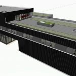
The base configuration of many of our systems can be used, together with a inspection or measurement tool, as a fully automatic wafer inspection systems for 4″ – 300mm wafers. Depending on the amount of loading stations our IL C3200, IL C3400 & IL C3800 can be used as an „EFEM – Equipment Front End Module“, which fully automatically transferrs the wafers from the cassettes to the inspection chamber. Each EFEM can be equipped with with differend kind of handling such as vacuum-, edge grip- and frame-handling. In addition many optional features such as class1 mini environment, SECSII/GEM interface, pattern recognition systems or reading cameras can be added to the base model.
Inspection of Wafer Frontside and Wafer Backside
The wafer will be checked for scratches, particles and inclusions. There is either a manual or a automatic movement of the wafer available. For the detection of all kind of surface defects different light modes such as bright field and dark field lightning are included in our systems.
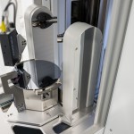
Inspection of the Wafer Edge
The inspection of the wafer edge will be done with a 4-axis turning module which helps to look on the edge from different view angles. In this way it’s possible to detect all kind of defect at the entire wafer edge w/o exclusion zone.
Inspection of Cracks and Defects before Polishing / after Dicing
With an optical inspection device local cracks, defects and inclusions in and on a wafer can be detected. Defect areas can be automatically inked and in the following step removed. In this way the amount of rejected chips can be reduced a lot which helps to improve the production yield.
NEWS