
")
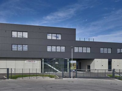
New Headquarters in Inning am Ammersee
In September 2018 the InnoLas Semiconductor GmbH moved to the new headquaters in Inning am Ammersee. With more than 400 square meters of cleanroom the production... Read More
InnoLas supports the charity organization OXFAM
The InnoLas Semiconductor GmbH started to support the global charity organization “Oxfam” financially in December 2017. The organisation is focused on the alleviation of global... Read More

Ground-Breaking! New Headquarters in Construction
Due to our limited production and storage area as well as separate production and office buidlings the InnoLas Semiconductor, GmbH builds a new headquarters in... Read More

Report – Semicon Japan 2016
The Semicon show in Japan took place in the Big Sight exhibition centre from 14.-16. December 2016. In total five halls were completely packed with companies... Read More

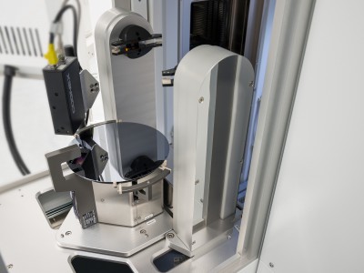
New Cooperation with ISRA Vision Systems AG
Together with the ISRA Vision Systems AG a fully automated wafer inspection system has been developed, assembled and commissioned. The automated wafer transfer between cassette... Read More

Semicon China from 15.-17.03.2016 in Shanghai
As the past few year InnoLas Semiconductor will participate at the Semicon show in China. The date of the exhibition is 15. – 17.03.2016 at... Read More
Further product diversification
For many years we used edge grip components for 300mm wafers. From now on all of our machines can be equiped with optional edge grip... Read More